HDL Works

- Home
- Products
- Sales
- Support
- Company
- HDL Corner
HDL Works

February 2021, HDL Works announces the release and immediate availability of
ConnTrace 2.1,
the PCB / FPGA connectivity visualization and verification tool.
ConnTrace is a new and easy to use tool, to visualize and verify how components (including FPGAs) connect to each other on 1 or multiple PCBs. It can handle (rotated) connectors as well as shrouds on (through) a backplane. The PCB connection view shows traces for all signals that can be reached through the connectors. Filters and sorting allow you to concentrate on the potential problems.
FPGA pins with the same pin name and connected to the same net are now imported as a single net (with multiple pins connected). This reduces the number of nets created for an FPGA and thus improves performance. A pin label is added for power and ground pins. For Xilinx FPGAs the ‘...power_routed.rpt’ file is now processed to extract additional voltage information.
Microsemi and Lattice FPGA power and ground pins are added to the virtual
netlist.
Extract FPGA PullMode from FPGA pin data and show in tooltip.
The total number of nets created for the FPGA is reported in the console window.
Tooltips can be automatic (timed) or on demand by pressing the F1 key. The behaviour is set with the tooltip button in the main toolbar or the SHIFT F1 accelerator key.
Tooltips can be pinned to the screen by pressing the ‘p’ key or by clicking
on the pin when the tip is visible. The pinned tooltip will stay visible
until the current project is closed or when you press the ESC key (or
remove the pin). They can be moved on screen by dragging the header to the
desired location.
Text in the tooltip can be selected and copied to clipboard using the
<ctrl-c> key.
All views can now be sorted by clicking in the header section. When the view supports a primary and secondary sort order the last clicked header represents the primary sort key and previous one is the secondary sort key. All columns use numeric sorting like: a1, a2, a10 (instead of a1, a10, a2) and empty entries are moved to the bottom of the column.
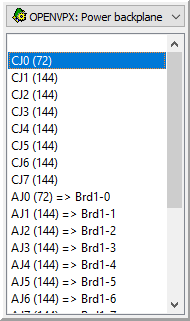
The connector selection widget in the connection dialog shows the unused connectors at the top of the list and appends (using ‘=>’) the connection name to the already used connectors. This makes it easier to see which connectors are still available.
A connection generator is added to bottom of the dialog to make it easier to create connections. The generator uses regular expressions. For one board you must specify an expression with a capture ‘()’ and the value of this capture ‘$1’ can occur in the Name and other boards (like shown below). When you press generate the found connections are added in the main connection table.


The order of schemas and visibility of the individual columns can be set with a
single dialog for both the Connection trace and Netlist view. The first board
cannot be moved. Other boards are moved by selecting the board and pressing the
↑U or ↓D button.
Use the buttons inside the ‘Visibility’ area to quickly hide or show specific
columns of all boards.
In the PCB netlist names all array indicator characters ‘[‘, ‘(‘ and ‘]’, ‘)’ are replaced with the ‘<’ and ’>’ characters (which have no meaning in regular expressions). When browsing for a PCB netlist name of a specific format the browse dialog shows the required file type in the dialog caption and uses a filename extension filter to reduce the number of visible files in the view.
A board which only contains connectors will now be treated as a netlist stub and no netlist analysis (like dangling wires or pullup/pulldown resistors) will take place but only voltage value extraction will be performed.
A separate format HdlWorksXML is added, which equals the format generated by HDL Works Altium Designer format, to be used when the generated netlist file is used on another system.
Pullup/pulldown resistors are now recognized for an IC pin which connects to a connector pin and contains a single resistor to either ground or power net.
Module verification is a new approach to verify connectivity of modules connected to the board, for which no netlist is available (like DIMMs or other memory modules) and of large components present in the netlist. Modules are defined in XML files and added to components as a virtual netlist. For more information about module verification please contact HDL Works.
A TCL based command line executable (named ‘conntrace_cmd’) has been added in this release. It can be used to create projects, add boards and FPGAs, create connections and rules. This TCL interface is not present in the GUI version of ConnTrace.
ConnTrace 2.1 is available now and can be downloaded and evaluated from the company website.
HDL Works develops and markets high-performance, intuitive tools for complex HDL design across a wide spectrum of applications. Its software products are available on Windows and Linux operating systems. HDL Works currently holds ConnTrace, EASE, HDL Companion and IO Checker in its product portfolio. Headquartered in Ede, The Netherlands, HDL Works is privately held.
HDL Works BV
###
ConnTrace, EASE, HDL Companion, IO Checker and Scriptum are trademarks of HDL
Works.
Copyright © 2004 - 2026 HDL Works