HDL Works

- Home
- Products
- Sales
- Support
- Company
- HDL Corner
HDL Works

November 2021, HDL Works announces the release and immediate availability of IO
Checker 4.2,
the FPGA and PCB IO verification tool.
IO Checker will verify that signal names used in the FPGA are connected to the appropriate signals on the PCB. Additionally it verifies the voltage values connected to the FPGA power and reference pins. IO Checker uses rules (based on regular expressions) to match the signals names in both the FPGA and PCB design environment. The rules can be generated automatically and be fine-tuned by the designer. The automated approach will often match 80% to 90% of all device pins.
The flexibility of IO Checker allows it to be used in any design flow and does not require any design methodology. The rules generator in combination with the sorted problem view allows engineers to validate a 1000+ pin device in half an hour.
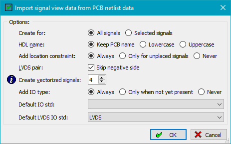
The way you can create constraints from PCB data is improved in two ways. In the import signal view from PCB netlist data dialog the option to only create signal view data for the selected signals in the Pin view has been restored. Secondly you can specify a default IO standard for both singled ended and LVDS signals.
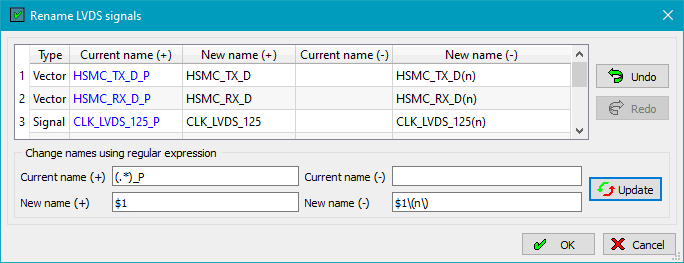
The new ‘Rename LVDS signals dialog’, activated through the ‘Tools’ menu, can be used to quickly edit groups of LVDS signals using regular expressions and create the constraint names you want to use. In the below example all _P post-fixes are removed and a new LVDS negative has been added with an (n) post-fix.
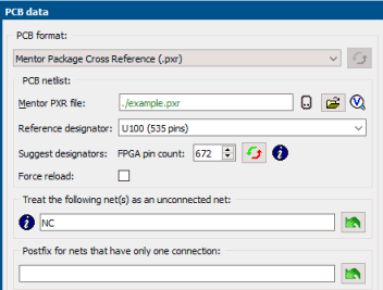
The expected FPGA pin count is now set on the PCB page of the project properties dialog. When pressing the ‘Suggest designators’ button IO Checker will search the netlist for reference designators with the specified pin count (using a margin). If you have specified a device on the FPGA device page, the pin count will be used here. The reference designator can always be specified manually.
The following changes have been made in the FPGA - PCB verification:
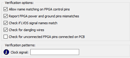
When the ‘Allow name matching on FPGA control pins’ is checked the matcher tries
to match the name of the FPGA pin and the PCB net name connected to this pin.
When unchecked no matching is done at all and you have to set a ‘Manual accepted
mismatch’ flag on the pin to match. For a new project this option is
not-checked. For existing projects it is checked to have the same match results
as in IO Checker 4.1.
The ‘Report FPGA power and ground mismatches’ check has been renamed. When not
checked mismatches are still shown in the PIN view, but not marked in the first
column and not reported in the report view.
In the verification patterns you can specify an expression for a ‘Clock’ signal
and IO Checker will check that each signal from the pin file that matches the
expression is mapped to a clock capable pin.
Fuzzy name matching for power/ground pins has been disabled.
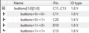
The Signal view now supports signals that have been defined using a 2
dimensional array.
In the properties dialog a dimension can be specified as [1:4]
(one dimensional) or as [1:2][0:7] (two dimensional).
Various usability improvements have been made in the Signal view:
Tooltips can be automatic (timed) or on demand by pressing the F1 key. The
behavior is set with the tooltip button in the main toolbar or the SHIFT F1
accelerator key.
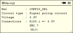
Tooltips can be pinned to the screen by pressing the ‘p’ key or by clicking on
the pin when the tip is visible. The pinned tooltip will stay visible until the
current project is closed or when you press the ESC key (or remove the pin).
They can be moved on screen by dragging the header to the desired location.
Text in the tooltip can be selected and copied to clipboard using the <ctrl-c>
key.
The netlist format for Altium Designer has been removed and replaced with HDL Works XML format. It is cumbersome to extract the XML netlist from Altium Designer using the command line. The HDL Works XML format is the same format, but generated using the Altium Designer IO Checker extension. Projects using the old format are automatically converted.
The Cadence PCB extraction file (from a board file) has been added as a separate format (Allegro PCB extract) to simplify its use.
A new netlist format based on CSV files has been added.
The project properties dialog shows an additional PCB option page when the PCB format is Cadence Allegro board or packaged netlist file(s) on which you can disable the voltage extraction. The generic EDIF and VeriBest EDIF netlist parsers have been deprecated.
IO Checker 4.2 is available now. Prices begin at € 750 or US$ 900. IO Checker can be downloaded and evaluated from the HDL Works website.
HDL Works develops and markets high-performance, intuitive tools for complex HDL design across a wide spectrum of applications. HDL Works currently holds BoardTrace, EASE, HDL Companion and IO Checker in its product portfolio. Headquartered in Ede, The Netherlands, HDL Works is privately held.
HDL Works BV
###
ConnTrace, EASE, HDL Companion, IO Checker and Scriptum are trademarks of HDL
Works.
Copyright © 2004 - 2026 HDL Works