The Pin view has been extended with 2 icon columns denoting the pin type derived from the FPGA pin file and the alternate device pin type (when set).
This makes it easier to see if a pin changed behaviour after pin mapping or if the alternate device pin has a different functionality.
The pin icons shown in the pin view and in the device view have been synchronized.
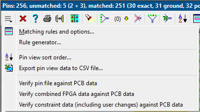
Both Pin- and Signal view toolbars have been extended with a menu and status button.
When errors are present a red cross is shown in the status button.
The menu button lists functionality available from the main menu bar to simplify access to actions available for the specific view.
Pin view toolbar menu
Signal view
The Signal view has been extended with an error column to either show a red/orange error/warning dot.
A tooltip in that column shows the related warning or error message(s).
Incorrect pin numbers or IO standards are drawn in the error color (red by default).
Device view
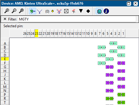
Added a functional name filter to the button bar. When active, only pins whose label contains the filter text are shown.
When a selection is present draw the not selected pins opaque. This makes it easier to see where the selected pins are located.
Drag & drop:
Do not select the first pin when it is not a valid drop target.
Take in account the IO standard (when set) during the drop.
Show a float window with the scheduled drop results
The ESC key now deselects all pins in the view.
Device view
Verification
The verification choices have been simplified and the verification wizard has been removed.
The default verification mode is changed to automatic, meaning that IO Checker will select the most appropriate verification mode based on the available data.
The severity of the IO Checker verification messages can now be set in the project properties dialog.
Verification has been improved for pins which are a dedicated LVDS pair.
Two new checks are added:
IOC-55: Check if analog ground pins and regular ground pins are not connected to the same PCB net.
IOC-57: Check if analog power pins and regular power pins are not connected to the same PCB net.
Symbol tool
Improvements in the Symbol tool:
Generic table search and replace dialog in the Pin view
Extended context menu of columns in the Pin view which have a fixed number of allowed entries.
Font selection for the labels shown the Symbol view
Context menu keyboard button support in the Symbol view
Wiring tool
Improvements in the wiring tool:
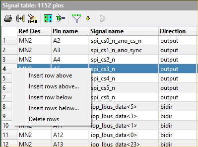
A context menu has been added to the vertical header to add/delete rows.
A generic table search and replace dialog
An option was added to remove wires from Cadence System Capture diagrams.
Wiring tool: row context menu
FPGA vendor and device support changes
Altera
Device updates for Agilex 3, Agilex 5, Agilex 7.
AMD
Device updates for Spartan Ultrascale+ and Versal Gen 2.
Efinix
Devices updates for Titanium.
Improved Efinix pin file reader to recognize 3 digits voltages (0.95 V)
Lattice
Device updates for Avant and Certus-N2
Microchip
Device updates for PolarFire and PolarFire-Soc.
The constraint file parser and generator now support DriveStrength and SlewRate properties.
Changed bank names in IGLOO2, SmartFusion2 and RTG4 devices from B<no> to Bank<no>
Enhancements
Use Shift+F11 to enable/disable timed tooltips (instead of Shift+F1)
Added option 'Existing wires: Replace/remove' in Cadence System Capture wiring.
Performance improvement when selecting a huge number of pins (but not all pins) in the device view.
In GUI and (verification) messages use "IO standard" instead of "IO type".
Generated HTML now also contains the signal view verification results.
Problem fixes
Id 2394: CSV export for pin view failed in certain cases if there was no pin file present.
Id 2393: If a pin used in the signal view does not exist on the device the verification message will now contain quotes around the pin name so it will be easier to see if the pin name contains leading or trailing whitespace.
Id 2391: A right mouse click in the device view would always deselect all pins besides the one under the mouse.
Id 2369: Report result summary after Import signal view data from FPGA/PCB data.